TMS320F28335ZHHA-Texas Instruments
$130.00
- تفصیل
- انکوائری
تفصیل
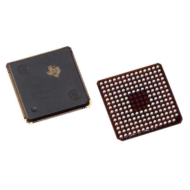
The TMS320F28335ZHHA device sold by xt-shenzhen is a high-performance microcontroller chip developed and designed by Texas Instruments. The device meets all the requirements of an automotive-grade chip, and has been widely recognized by major automakers around the world in terms of processing speed and product quality. If you want to know more original Texas Instruments chips, please contact xt-zhenhen company to serve you! ! !

TMS320F28335ZHHA adopts Harvard (Harvard) bus architecture design. When encountering equipment failure, it can quickly interrupt the response and processing to better protect equipment safety. The high-performance static CMOS technology of the TMS320F28335ZHHA enables device frequencies up to 150MHz (6.67ns cycle time). This series of products has developed a variety of packaging forms to meet the various application environments of customers, and is very suitable for customers who want to develop systems independently.

• High-performance 32-bit CPU (TMS320C28x)
– IEEE 754 single-precision floating-point unit (FPU) (F2833x only)
– Efficient code (using C/C++ and assembly language)
• 6-channel DMA controller (for ADC, McBSP, ePWM, XINTF and SARAM)
• 16-bit or 32-bit external interface (XINTF)
• On-chip memory
• Boot ROM (8K × 16)
– Has software boot mode (via SCI, SPI, CAN, I2C, McBSP, XINTF, and parallel I/O)
– Standard Math Tables
• Clock and system control
– On-chip oscillator
– Watchdog Timer Module
• GPIO0 to GPIO63 pins can be connected to one of eight external core interrupts
• Peripheral Interrupt Expansion (PIE) module supporting all 58 peripheral interrupts
• 128-bit security key/lock
– Protect flash/OTP/RAM blocks
– Prevent firmware reverse engineering
• Enhanced control peripherals
– Up to 18 PWM outputs
• Three 32-bit CPU timers
• Serial peripherals
– One SPI module – 1 Inter-Integrated Circuit (I2C) bus
• 12-bit ADC, 16 channels
–80ns conversion rate
–2 × 8 channel input multiplexer
– Twice sample and hold
– Single/simultaneous conversion
– Internal or external benchmarks
• Up to 88 individually programmable multiplexed GPIO pins with input filtering
• Supports JTAG boundary scan
– IEEE Std 1149.1-1990 Standard Test Access Port and Boundary Scan Architecture
• Advanced debugging features
– Analysis and breakpoint functions
– Hardware real-time debugging
• Development support includes
–ANSI C/C++ compiler/assembler/linker
– Code Composer Studio™ IDE
–DSP/BIOS™ and SYS/BIOS
– Digital Motor Control and Digital Power Software Libraries
• Low power mode to save energy
– Support idle, standby, shutdown modes
– Disable individual peripheral clocks
• AEC Q100 certified for automotive applications

| frequency | 150میگاہرٹز |
| بجلی کی سپلائی (ڈی سی) | 1.80وی (min) |
| پنوں کی تعداد | 179 |
| Clock frequency | 150میگاہرٹز |
| رام سائز | 68KB |
| ہندسوں کی تعداد | 32 |
| فلیش میموری کی گنجائش | 512KB |
| Number of UARTs | 3 |
| ینالاگ سے ڈیجیٹل کنورژن (اے ڈی سی) | 16 |
| ان پٹ/آؤٹ پٹ کی تعداد | 88 Input |
| آپریٹنگ درجہ حرارت | -40℃ ~ 85℃ |
| پاور سپلائی وولٹیج (زیادہ سے زیادہ) | 1.995وی |
| پاور سپلائی وولٹیج (کم از کم) | 1.805وی |
| تنصیب کا طریقہ | سطح کا پہاڑ |
| پیکج | BGA-179 |
| پیکنگ | ٹرے |

