
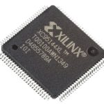
XC7Z045-2FFG676I-original Xilinx

- Description
- Inquiry
Description
XT-ShenZhen pays attention to popular models and adjusts inventory in time for customers to purchase! The XC7Z045-2FFG676I device is a PSoC/MPSoC microprocessor from Xilinx. The device belongs to the Zynq-7000 programmable SoC family. It can serve a very wide range of applications. XT-ShenZhen has a stock warehouse, and a variety of models are fully stocked. Welcome to contact us for more information!

The Zynq-7000 family has the flexibility and scalability of FPGAs, but also provides the performance, power and ease of use for ASICs and ASSPs. The Zynq-7000 family of devices enables designers to leverage industry-standard tools for low-cost and high-efficiency applications. Although every device in the Zynq-7000 series contains the same PS, the PL/I/O resources are different among PL/I/O devices.
The XC7Z045-2FFG676I device makes the system unique and differentiated. The combination of PS and PL can be a two-chip solution such as ASSP (such as ASSP and FPGA), which is unmatched in limited I/O bandwidth, latency and power consumption. Xilinx provides many soft IPs for the Zynq-7000. In PS and PL, standalone and Linux device drivers are available. The development environment of the Vivado® Design Suite supports the rapid development of software, hardware and systems engineers.

Based on ARM Cortex-A9
Application Processor Unit (APU)
• 2.5 DMIPS/MHz per CPU
• CPU frequency: up to 1 GHz
• Consistent multiprocessor support
• ARMv7-A architecture
• TrustZone® security
• Thumb®-2 instruction set
• Jazelle® RCT Execution Environment Architecture
• NEON™ media processing engine
• Single- and double-precision Vector Floating Point Units (VFPUs)
cache
• 512 KB 8-way set-associative L2 cache (shared between CPUs)
• 256 KB on-chip RAM (OCM)
• 8-bit SRAM data bus supporting up to 64 MB
• ONFI1.0 NAND Flash support (1-bit ECC)
• 1588 rev approval. 2 PTP frames
• GMII, RGMII and SGMII interfaces
• USB 2.0 Compliant Device IP Core
• 8-bit ULPI external PHY interface
• Two SD/SDIO 2.0/MMC3.31 compliant controllers
• Two high-speed UARTs (up to 1 Mb/s)
• Two master-slave I2C interfaces
• High bandwidth connections within PS and between PS and PL

| RAM size | 256 KB |
| Number of pins | 676 |
| Installation method | Surface Mount |
| Number of pins | 676 |
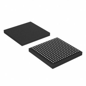
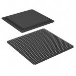
| Package | FCBGA-676 |
| Operating temperature | -40℃ ~ 100℃ (TJ) |
| Product Lifecycle | Active |
| Packing | Tray |