
DSPIC33EP128GP502-E/SS – Microchip


$61.80
- Description
- Inquiry
Description
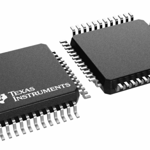
The DSPIC33EP128GP502-E/SS device is a 16-bit microcontroller (MCU) developed by Microchip Semiconductor Corporation.

| RAM Memory Size | 8K x 16 |
| Number of Bits | 16 |
| Number of ADCs | 1 |
| Operating Temperature (Max) | 125 ℃ |
| Operating Temperature (Min) | -40 ℃ |
| Mounting Style | Surface Mount |
| Case/Package | SSOP-28 |
| Operating Temperature | -40℃ ~ 125℃ |
| Product Lifecycle Status | Active |
| Packaging | Tube |
| RoHS | RoHS Compliant |

Operating Conditions
- 3.0V to 3.6V, -40°C to +85°C, DC to 70 MIPS
- 3.0V to 3.6V, -40°C to +125°C, DC to 60 MIPS
Core: 16-Bit dsPIC33E/PIC24E CPU
- Code Efficient (C and Assembly) Architecture
- Two 40-Bit-Wide Accumulators
- Single Cycle (MAC/MPY) with Dual Data Fetch
- Single-Cycle, Mixed-Sign MUL plus Hardware Divide
- 32-Bit Multiply Support
Clock Management
- 1.0% Internal Oscillator
- Programmable PLLs and Oscillator Clock Sources
- Fail-Safe Clock Monitor (FSCM)
- Independent Watchdog Timer (WDT)
- Fast Wake-up and Start-up
Power Management
- Low-Power Management modes (Sleep, Idle, Doze)
- Integrated Power-on Reset and Brown-out Reset
- 0.6 mA/MHz Dynamic Current (typical)
- 30 μA IPDCurrent (typical)
High-Speed PWM
- Up to Three PWM Pairs with Independent Timing
- Dead Time for Rising and Falling Edges
- 7.14 ns PWM Resolution
- PWM Support for:
– DC/DC, AC/DC, Inverters, PFC, Lighting
– BLDC, PMSM, ACIM, SRM
- Programmable Fault Inputs
- Flexible Trigger Configurations for ADC Conversions
Advanced Analog Features
- ADC module:
– Configurable as 10-bit, 1.1 Msps with four S&H or
12-bit, 500 ksps with one S&H
– Six analog inputs on 28-pin devices and up to
16 analog inputs on 64-pin devices
- Flexible and Independent ADC Trigger Sources
- Up to Three Op Amp/Comparators with
Direct Connection to the ADC module:
– Additional dedicated comparator
– Programmable references with 32 voltage points
- Charge Time Measurement Unit (CTMU):
– Supports mTouch™ capacitive touch sensing
– Provides high-resolution time measurement (1 ns)
– On-chip temperature measurement
Timers/Output Compare/Input Capture
- 12 General Purpose Timers:
– Five 16-bit and up to two 32-bit timers/counters
– Four Output Compare (OC) modules, configurable
as timers/counters
– PTG module with two configurable timers/counters
– 32-bit Quadrature Encoder Interface (QEI) module,
configurable as a timer/counter
- Four Input Capture (IC) modules
- Peripheral Pin Select (PPS) to allow Function Remap
- Peripheral Trigger Generator (PTG) for Scheduling
Complex Sequences
Communication Interfaces
- Two UART modules (17.5 Mbps):
– With support for LIN/J2602 protocols and IrDA
®
- Two 4-Wire SPI modules (15 Mbps)
- ECAN™ module (1 Mbaud) CAN 2.0B Support
- Two I2C™ modules (up to 1 Mbaud) with SMBus Support
- PPS to allow Function Remap
- Programmable Cyclic Redundancy Check (CRC)
Direct Memory Access (DMA)
- 4-Channel DMA with User-Selectable Priority Arbitration
- UART, SPI, ADC, ECAN, IC, OC and Timers
Input/Output
- Sink/Source 12 mA or 6 mA, Pin-Specific for Standard VOH/VOL, up to 22 or 14 mA,respectively for Non-Standard VOH1
- 5V Tolerant Pins
- Peripheral Pin Select (PPS) to allow Digital Function
Remapping
- Selectable Open-Drain, Pull-ups and Pull-Downs
- Up to 5 mA Overvoltage Clamp Current
- Change Notification Interrupts on All I/O Pins
Qualification and Class B Support
- AEC-Q100 REVG (Grade 1, -40°C to +125°C) Planned
- AEC-Q100 REVG (Grade 0, -40°C to +150°C) Planned
- Class B Safety Library, IEC 60730
Debugger Development Support
- In-Circuit and In-Application Programming
- Two Program and Two Complex Data Breakpoints
- IEEE 1149.2 Compatible (JTAG) Boundary Scan
- Trace and Run-Time Watch