
How are semiconductor memory chips classified?
In daily life, we often use U disk, TF card, SD card, hard disk, etc. to store some data information. Modern storage technology is mainly divided into three parts, namely magnetic storage, optical storage and semiconductor storage.
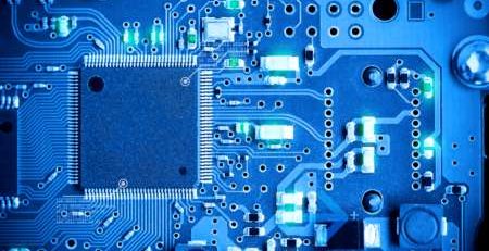
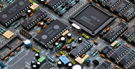
Semiconductor memory is the memory with “semiconductor integrated circuit” as the storage medium, such as the U disk or SSD hard disk we usually use, which is full of PCB circuit boards and various components. Among them is a “memory chip”, which is dedicated to storing data.
Compared with traditional magnetic disks (such as HDD hard disks), semiconductor memory is lighter in weight, smaller in size, and faster in reading and writing. In recent years, the whole society has paid great attention to the chip semiconductor industry. But what everyone mainly cares about is computing chips such as CPU and GPU. In fact, the memory chip is also a very important device.
Semiconductor memory can also be divided into volatile (VM) memory and non-volatile (NVM) memory in detail. Volatile memory cannot retain data when the device is powered off, while non-volatile memory can. Many materials now also divide semiconductor memory into random access memory (RAM) and read only memory (ROM). ROM Read-only memory is readable but not writable. RAM random access memory can randomly read or write data from any location in memory.
 Volatile memory (VM) is mainly divided into DRAM (Dynamic Random Access Memory, dynamic RAM) and SRAM (Static Random Access Memory, static RAM):
●DRAM consists of many repeated bit cells (Bit Cell), each basic cell consists of a capacitor and a transistor (also known as 1T1C structure). The amount of charge stored in a capacitor, used to represent “0” and “1”. There will be leakage due to capacitance. Therefore, periodic “dynamic” charging must be performed to maintain the potential before data changes or power outages. Otherwise, data will be lost. Therefore, DRAM is called “dynamic” random access memory.
●The structure of SRAM is much more complicated than that of DRAM. The basic unit of SRAM consists of at least 6 transistors: 4 FETs (M1, M2, M3, M4) form two cross-coupled inverters, and 2 FETs (M5, M6) are used to read and write bit lines. The control switches (bit lines) form latches (flip-flops) through these FETs and latch the binary numbers 0 and 1 when powered.
Therefore, SRAM is called “Static Random Access Memory”.
SRAM does not need to be refreshed regularly and has fast response speed, but it consumes a lot of power, has low integration and is expensive.
Therefore, it is mainly used for the first-level cache and the second-level cache of the CPU. Also, it will be used in FPGAs.
Non-Volatile Memory (NVM)
There are many technical routes for non-volatile storage products, which is the ROM mentioned above.
The oldest type of ROM, all about reading data. The storage content is fixed at the factory and cannot be modified. Later, experts invented PROM (Programmable ROM, programmable ROM). Such ROMs can usually only be programmed once. When shipped from the factory, all memory cells are set to 1. Using special equipment, the fuse can be blown by current or light (ultraviolet light) to achieve the effect of rewriting the data. PROM is more flexible than ROM. But with the breakthrough of technology, experts invented EPROM (Erasable Programmable, erasable programmable ROM). Can be erased with light and electricity, although electricity is more convenient. Electrically erasing is called EEPROM (Electrically Erasable Programmable EEPROM).